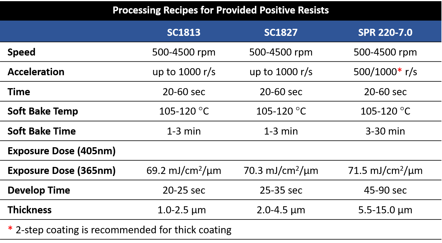
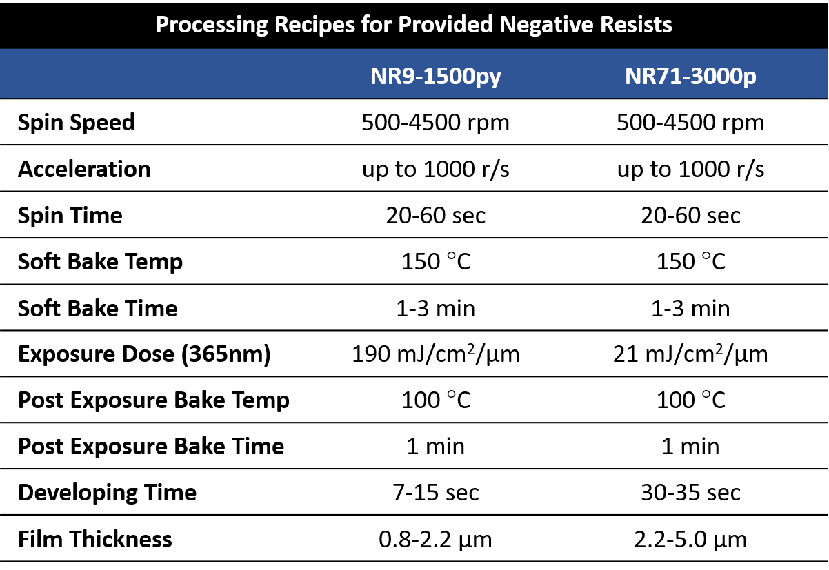
This section contains the information and standard recipes for the Photoresists and the Alignment & Exposure Tools that are available at GT IEN cleanrooms. The information can be used as a reference to design a process flow. Please refer to this link for further information on Resists.
On Contact Mask-Aligner
- Positive Resists (cleanroom supplied)

- Negative Resists (cleanroom supplied)

(Back to Top)
On Direct Laser Writer
- Configured for topside and backside alignment, capable of processing up to 6” wafers
- Available Wavelengths: 365 nm & 405 nm
- Configure for topside alignment, capable of processing up to 6” wafers
- Available Wavelengths: 365 nm & 405 nm
- Configured for topside and backside alignment of 4” wafers
- Available Wavelength: 365 nm
- Used to expose resist on photomask plates, wafers and other substrates up to 8" x 8" in size. Capable of direct writing, grayscale lithography, and SU-8 exposure.
- Available wavelengths: 375 & 405 nm
- 1um minimum feature size
- Linewidth Variation: 120 nm
- Alignment Accuracy: 500 nm
- Substrate size: pieces up to an 8”x 8” substrate

The exposure time can be calculated by taking the dosage (found on the photoresist datasheet) and dividing it by the intensity measured of the exposure tool. If possible, the intensity can be measured through the mask. If there is not a large enough Clearfield space to accommodate the sensor, subtract 1.0 mW/cm2 for a 405 nm exposure to account for the intensity lost traveling through the mask. Subtract 0.7 mW/cm2 for 365 nm. The intensity loss can vary depending on the mask material, so that value should be looked up before exposure if unable to measure through the mask.
(Back to Top)