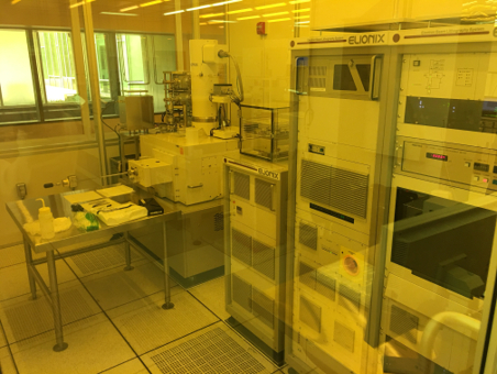
Georgia Tech’s Institute for Electronics and Nanotechnology (IEN) currently operates an Elionix ELS-G100 100kV electron beam lithography system. The Elionix ELS G-100 is a high-speed, ultra high-precision thermal field emission (TFE) electron beam lithography system.
Ultra fine line lithography
The ELS G-100 is capable of generating patterns with a line width of 6nm. The system provides a stable 1.8nm electron beam using high beam current at 100kV. The fine line patterns can be drawn using commercially available resists.
Ultra high beam position accuracy with laser interferometer stage
The highly precise stage that the ELS G-100 employs is based on over 35 years of expertise with lithography systems. A 20bit DAC provides high beam positioning resolution. In addition, the laser interferometer with its reading resolution of 0.31nm enables a stitching accuracy of 15nm and overlay accuracy of 20nm.
Uniform fine pattern writing over entire field
Significantly small distortion enables uniform and stable fine pattern writing over large writing fields. Uniform 10nm lines can be drawn from the edge to the edge of a 500μm field without stitching. At a beam current of 1nA, 20nm lines can be written over an entire 500μm field without stitching. No stitching guarantees accuracy and eliminating the need for stage movement enhances writing speed.