Equipment Description
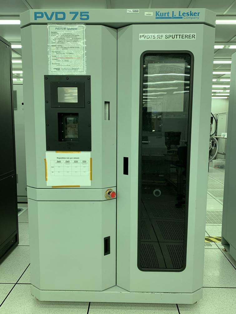
The RF sputterer can be used to deposit many dielectrics. Coatings are performed by accelerating ions or an argon oxygen mixture into the surface of a sputter target, which is made of the material to be applied to the sample. -Sputter two or more dissimilar materials simultaneously for complete control of film stoichiometry (co-deposition) -Max RF power 325W -Integrated touch screen control -Single substrate up to 12" diameter -Multiple substrate up to 4" diameter -Substrate fixture rotation up to 20rpm
Standard Metal Materials Available:
Manufacturer: Kurt J. Lesker
| Institute |
Georgia Tech |
| Department |
IEN - Micro/Nano Fabrication Facility |
Sub Tool Of  |
Marcus Inorganic Cleanroom |
| |
|
| Applications |
Pilot production
• Optical coatings
• Metal coatings
• Nanotechnology
• OLEDs
• Protective coatings |
Machine Specifications and Data:
Power Specifications:
- RF power supply
- Miscellaneous note
- Maximum Current for DC Sputtering:
- Maximum Power for RF Sputtering: 325 W
- Maximum Temperature for Substrate Heater: