Dry Etch vs Wet Etch
Etching is used in Micro-fabrication to chemically and physically remove layers from the surface of a wafer during manufacturing. The cleanrooms at IEN carry a multitude of tools which can be used for a wide variety of etching processes including dielectrics, substrates, and metal etching.
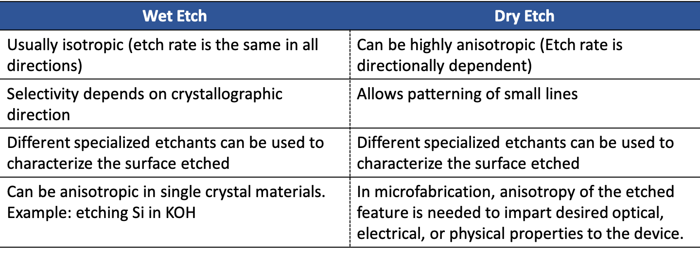
Wet Etching
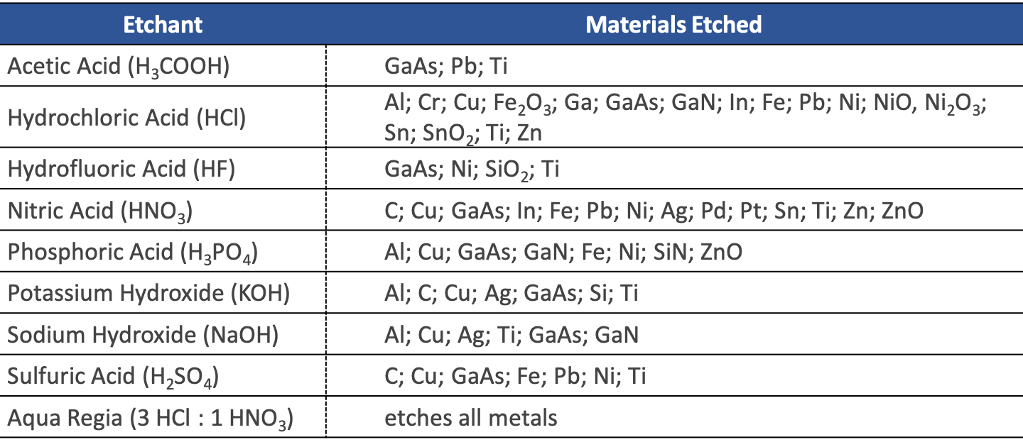
Wet etching Utilizes liquid chemicals to dissolve selected materials from a substrate. Many materials are etched isotropically while others etched anisotropically in certain chemicals. Users must process in a well-ventilated fumehood with proper personal protection equipment. Many processing steps require mixing liquid chemicals together. Users should make themselves aware of the chemical reactions possible when mixing chemicals in order to minimize the risk to themselves and others around them. For example, always add acids to water because adding water to an acid causes a highly exothermic reaction which can cause a fire and release dangerous gases into the air. Please use the tables below with care.
Dry Etching
Dry etching utilizes gas-phase chemicals or plasma to remove selected materials from a substrate. The IEN provides four dry etching capabilities: Vaporized chemical etching, Reactive Ion Etching (RIE), Inductively Coupled Plasma (ICP) Etching and Laser Etching.
- Substrate Material:
- Semiconductors: Si, III-V compounds
- Dielectric: SiO2, SiN, Quartz, Glass, TiO2, TiN, etc
- Metal: Al, Cr, Ti, Mo, W
- Ceramic
- Polymer
- Substrate Size: 4" wafer or small piece
- Etching Techniques:
- Dry/Vapor Chemical Etching:
- XeF2 dry etching
- HF vapor etching
- RIE Etching:
- F-based chemistry: SF6, CF4, CHF3, C4F8
- Cl-base chemistry: Cl2, BCl3
- DRIE/ICP Etching:
- Bosch Process F-based chemistry: SF6, CF4, CHF3, C4F8
- Cl-base chemistry: Cl2, BCl3
- Special chemistry: HBr
- Laser Etching:
- Femtosecond laser, 1030 nm wavelength, 221 fs minimum
- Nd-YLF laser @16W, 1064nm/524nm wavelength
- UV laser, 355 nm wavelength
- CO2 laser @60W, 1060 nm wavelength