Different Methods for SiO2 Deposition/Growth
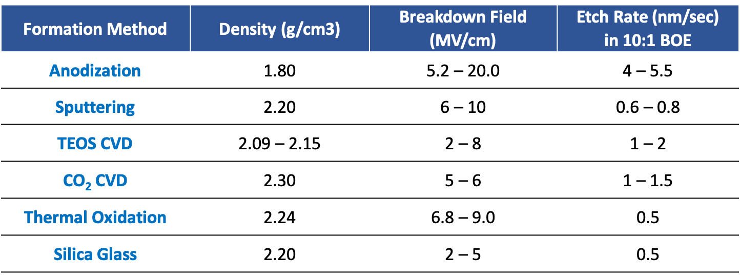
Silicon Dioxide Property Comparison
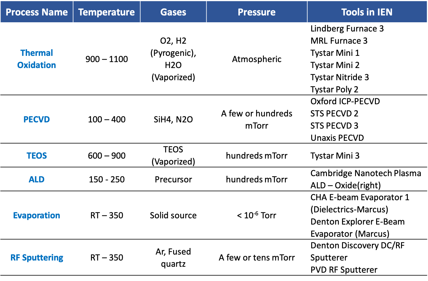
Silicon Dioxide Deposition/Growth Techniques @ IEN
Thermal Oxidation:
In microfabrication, thermal oxidation is a way to produce a thin layer of silicon dioxide (SiO2) on the surface of a silicon wafer and is performed in furnaces. This technique forces an oxidizing agent to diffuse into the wafer at high temperature and react with it. The rate of oxide growth is often predicted by the Deal-Grove model. Dry oxidation is slower than wet oxidation due to oxygen’s slower rate of diffusion through the silicon dioxide layer to the silicon/oxide interface where the oxidation reaction occurs. Wet oxidation is used for growing thicker (> 100 nm) layers of silicon dioxide for applications such as isolation (field oxides and local oxidation) and dopant diffusion barriers, in which oxide quality is less important.
PECVD:
In most PECVD configurations, the gas flows out of the anode, or showerhead, where it is ionized by the RF power, creating a plasma. The substrate is located on the cathode, or platen, of the system. Because the surface of the substrate has a slightly positive charge, the slightly negative gas ion is an attracted to the surface. The heat of the cathode that the substrate rests on, removes the by-products by desorption. These by-products are then removed from the process chamber by the vacuum pump.
TEOS:
TEOS (Tetra-ethyl-orthosilicate) is a colorless liquid at room temperature. For TEOS LPCVD process, the vapor may be brought to the reaction chamber using either a bubbler or a liquid injector. In a TEOS CVD process, TEOS is delivered mostly using an inert carrier gas to a reaction chamber heated to a temperature between 650 and 850 °C. TEOS molecules are dissociated and adsorbed onto the wafer surface. The neighboring ethyl alkyl groups then interact with each other to form stable products, which then detach from the surface and leave behind a -O-Si-O- link to the surface. Although TEOS is an excellent source of oxygen atoms by itself, adding O2 gas increases the deposition rate. N2 is the most popular choice for the carrier gas.
ALD:
A film is grown on a substrate by exposing its surface to alternate gaseous precursors. The precursors are injected into processing chamber as a series of sequential, non-overlapping pulses. In each of these pulses the precursor molecules react with the surface in ideally, a self-limiting way, so that the reaction terminates once all the reactive sites on the surface are consumed. For process that are not self-limiting, the precursor pulse length must be precisely controlled. Consequently, the maximum amount of material deposited on the surface after a single exposure to all the precursors is determined by the nature of the precursor-surface interaction. By varying the number of cycles, it is possible to grow materials uniformly and with high precision on arbitrarily complex and large substrates.
Evaporation:
Silicon dioxide can be deposited by using e-beam evaporation technique. The e-beam at low power can sweep and uniformly fuse the source, and then evaporation proceeds. Unlike many other materials, silicon dioxide sublimates when it is evaporated. The deposited SiO2 films are expected to be smooth and amorphous with good adhesion.
Sputtering:
In sputterering, a plasma hits a target and deposits a dielectric layer. In most cases, the sputter target will be composed of the target material in the desired composition. It is also possible to use targets of the components of the desired material and combine them during deposition using a reactive sputterer. Since the dielectric target will accumulate a charge during the deposition process, a RF power generator is required.