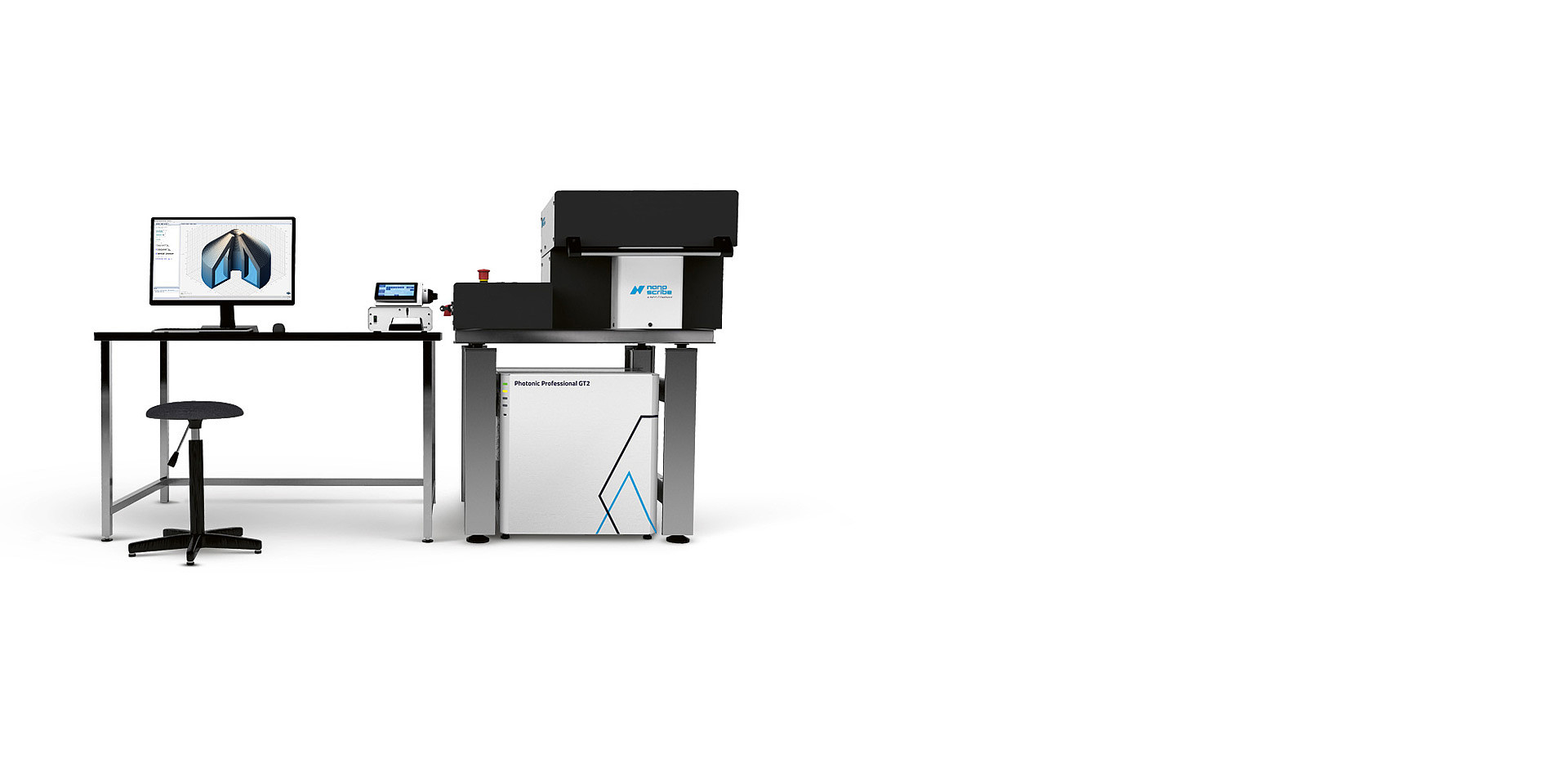
Nanoscribe GT2 Upgrade
Description: weblinkTechnology upgrades are designed for fast, high-precision 3D printing of objects and structures with sub micron details. Increased scan speeds significantly reduce print times by a factor of 10 without sacrificing quality. For example, a 1cm x 1cm x 500um print that normally took 96 hours to print can now be completed in fewer than 10 hours. Sub micron print resolution can now print with details from 160nm up to the millimeter range. The new IP-Q Photo Resist means that the maximum print size in the Z direction is now 8mm while maintaining the accuracy 2 Photon Polymerization provides. This will greatly aid in rapid prototyping of microfluidic designs, like microfluidic chambers. We hope this new technology will greatly aid researchers who are working in engineering
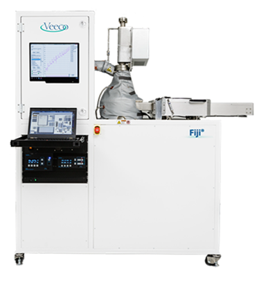
Veeco FiJi ALD Gen II
Description: weblinkThe purchased Veeco Fiji G2 ALD system is dedicated for photovoltaic and photonics applications which require contamination free environment The system is equipped with autoload sample chuck, turbo pumps on both chamber and load-lock, and sapphire plasma tube which enables it to produce high quality nitride. It will greatly help the research projects of Prof. Rohatgi and Prof. Adibi's group. The tool is also available to all cleanroom users (internal and external) with similar research interests.
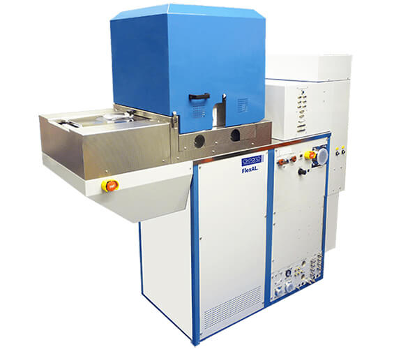
Oxford Instrument Flex ALD
The FlexAL atomic layer deposition (ALD) system offers a broad range of optimized high-quality plasma ALD and thermal ALD processes with maximum flexibility in precursors, processes gases, and hardware configuration within a single process chamber.
1) Remote plasma for low damage plasma ALD combined with thermal ALD in one deposition chamber
2) RF biased electrode option available for control of film properties
3) Industry-standard cassette to cassette handling for higher throughput
4) Maximum flexibility in the choice of precursors, process gases, hardware features and options
5) Optimized to maintain low-damage, high quality substrates
6) Removable liners allow for easy chamber maintenance
7) Low temperature to enable high-quality deposition on temperature-sensitive surfaces.
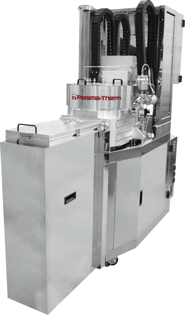
Plasma-Therm Dielectric ICP
Plasma-Therm’s Takachi is a robust Inductively Coupled Plasma (ICP) system designed for a wide range of uniform, high-quality ICP etch applications. With its multiple film etching film capabilities, this unique system has the ability to etch dielectrics (SiNx, SiO2, a-Si, SiOxNy, SiC, Ta2O5), polymers (photoresist, polyimide, BCB), conduct surface treatment (O2 modification of PSS) and surface texturing of Solid-State Lighting and Solar cells, and descum wafers. This system will satiate the increased demand for dielectric and polymer etching systems in our facilities. Handling
• Load lock with easy 4-button control for continuous processing
• 254mm platen provides adequate load capacity for all applications
• Temperature control of electrode with liquid-to liquid heat exchanger
• 300W, 13.56 MHz electrode (600W optional)
• 1kW 2MHz inductive ICP source (2kW optional)
• 4 MFCs standard (20 optional) – Gas box is tool mounted or remote
• Compact footprint (<1.0 m2)
• Best-of-breed components for fast availability of parts
• CE/UL compliant • Robust design with high reliability Software:
• Industrial PC-based, Cortex® control system
• Endpoint on multi-layer stacks
• Achieve target etch depths
• Run-to-run repeatability (< ± 2% variation w/Endpoint)
• Optical Emission Spectroscopy (OES)
• System-based inputs such as RF match positions, throttle valve position